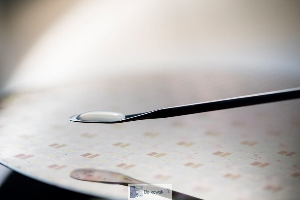
Baikowski® develops oxide CMP solutions precisely engineered for applications where precision and/or selectivity in material removal are critical—such as electronic components and semiconductors.
View polishing related products
✅ What is a CMP process?
CMP (Chemical Mechanical Polishing/Planarization) is a highly precise polishing process. It combines two specific actions.
- Chemical interaction: Substrate modification through dedicated chemical agents
- Mechanical action: Engineered abrasive particles working in conjunction with polishing pads and slurry
✅ Why CMP is Critical in Electronics & the Semiconductor Industries?
Experts recommend chemical mechanical planarazing for highly demanding semiconductor applications, like integrated circuits or memory disks for example. Indeed, the process brings remarkable properties:

- High precision: the more data we achieve to store on a device, the more precise the design becomes. Storage devices are often produced by successive layers deposit. Those layers are very thin and must be fully flat with a perfect surface finish. Several means help measuring the surface finish, for example the Peak-to-Valley. Indeed, PV is the measurement of the height difference between the highest point and the lowest point on the surface polished. The latest technologies of semiconductors require PV down to Angstrom levels (10-10m).
- Fast use: CMP is a multi-step process related to several substrates polishing. The objective is to optimize the duration of each step. However, keeping a high precision polishing process is still essential. Each step is already lasting less than a minute!
In conclusion, by removing surface roughness and precisely leveling layers and features, CMP enables:
- Denser integration: More transistors in less space
- Higher performance: Enhanced device capabilities
- Improved reliability: Better long-term product stability
✅What is Baikowski offering for CMP?
 We provide Diamond, Ceria & High Purity Alumina for CMP.
Silica polishing often involve ceria slurries (shallow trench isolation – STI CMP) for their:
- Crystallinity
- Shape
- Particle size
- Particle size distribution
- Phasic purity, which is highly controlled
Moreover, decades of experience in customizing polishing solutions for semiconductor applications have built extensive process knowledge. This expertise enables:
- Superior control over milling and dispersion
- Improved selectivity, consistent material removal rates, and reduced defect density across demanding semiconductor CMP applications.
✅FAQ
How do I choose between alumina (HPA) and silica for my CMP process?
- Use alumina (HPA) when you need higher material removal rates, particularly on metals like tungsten (W) or aluminum (Al) with appropriate chemistry.
- Choose silica when a softer, finishing-grade action is required for smooth, uniform surfaces.
- Consider our advanced oxide solutions to achieve tight selectivity requirements.
 Where can I find information on sapphire polishing?
 Where can I find information on sapphire polishing?
See our dedicated Sapphire Polishing CMP article with machine specifications, pad selection, flow rates, and comparative performance data.
It includes details on our three key SPH products:
- SPH-51 (silica): Optimized for polishing sapphire C and A planes with perfect surface finish
- SPH-53 (silica): Balanced throughput and surface quality
- SPH-9D (alumina): Very high removal rate on C-axis; suitable for double-face polishing
 When should I choose BRA15?
 When should I choose BRA15?
Select BRA15 alumina for semiconductor CMP steps requiring:
- Processing of metals (e.g., tungsten, aluminum)
- An α-phase design and narrow PSD in order to get consistent performance and reliable process control.
- Sustained material removal while maintaining finish quality
Can you customize oxide solutions for our specific process?
Yes. We tailor powder engineering (size, PSD, crystal structure/phase) and slurry formulation (pH, solids, additives, viscosity) to your tool-and-pad pairing to optimize MRR and surface integrity.
✅Next Steps
Ready to optimize your CMP process? Contact our team for:
- Product selection guidance
- Custom formulation development
- Process optimization support